
Until recently the easiest way to explain faster chips was simple: make the transistors smaller. That story is not over, but it is no longer the whole story. The next major leap in chip design may come from building upward.
The semiconductor industry is entering a new era, an era of innovation. The old marketing language still revolves around nanometers, nodes, and transistor density, but the real action is increasingly happening in the third dimension. Instead of only shrinking circuits across a flat piece of silicon, companies are stacking cache, bonding chiplets, moving power delivery to the backside of wafers, and experimenting with architectures that place memory and compute much closer together.
That may sound like a deeply technical shift, but the reason is easy to understand: modern chips are running into a data movement problem.
Moving information around a processor is becoming one of the most expensive things a chip can do. It costs energy. It creates heat. It adds latency. In AI systems, gaming CPUs, servers, and future laptops, performance is no longer just about how much raw compute a chip has. It is about how quickly and efficiently data can get to that compute without wasting power along the way.
That is why AMD’s 3D V-Cache, IBM’s new nanostack research, Intel’s Foveros Direct packaging work, and Qualcomm’s High Bandwidth Compute roadmap all point in the same direction. The future of chip design is not just smaller. It is taller, denser, and more memory-aware.
The Old Chip Story Was Simple: Smaller Meant Better
For most of the modern PC era, progress was easy to explain. A new manufacturing node arrived, transistors got smaller, chips became faster or more efficient, and consumers eventually saw the benefits in desktops, laptops, game consoles, phones, and servers.
That scaling model powered decades of progress. It gave us faster CPUs, more powerful GPUs, better smartphones, and cloud data centers capable of handling workloads that would have seemed impossible not that long ago.
But traditional scaling has become harder, more expensive, and less predictable. The industry can still make progress at advanced nodes, but every step now requires enormous investment, specialized equipment, and increasingly complex manufacturing techniques. Smaller transistors still matter, but they are no longer enough by themselves.
The bottleneck has shifted. In many workloads, the question is not only “how many transistors can we fit?” It is also “how efficiently can those transistors talk to memory, cache, power delivery, and each other?”
That is where 3D architecture comes in.
AMD 3D V-Cache Made Vertical Chip Design Real for Consumers
The easiest way to understand this shift is AMD’s 3D V-Cache.
AMD did not need to explain every detail of advanced packaging to make the idea land with regular buyers. The pitch was simple: stack extra cache on top of the CPU die, keep more data close to the processor cores, and improve performance in workloads that benefit from a larger cache pool. For gamers, that translated into a very real product category. Ryzen X3D chips became some of the most desirable gaming CPUs on the market because the extra cache could deliver strong real-world gains without requiring a completely different PC platform.
That is the important part. 3D chip design is not just a laboratory concept. It is already sitting inside consumer desktops.
In traditional chip design, everything competes for space across a mostly flat surface. If a company wants more cache, more cores, more I/O, or more specialized logic, it has to make difficult layout decisions. 3D stacking changes that equation by allowing some parts of the chip to move upward instead of only outward.
AMD’s approach shows why this matters. Cache is valuable because it keeps frequently used data close to the CPU. When the processor can pull from nearby cache instead of reaching farther out to system memory, it can reduce latency and improve performance in the right workloads. That is especially useful in games, where large pools of fast-access data can help smooth performance and improve frame rates.
It also gives consumers a useful mental model for the future. The next generation of chip improvements may not always look like higher clock speeds, more cores, or smaller nanometer numbers. Sometimes the improvement may come from smarter placement.
The Real Enemy Is Distance
At the chip level, distance is expensive.
Every time data moves from one part of a system to another, it costs time and energy. A CPU core reaching into cache is one thing. A GPU pulling data from high-bandwidth memory is another. A server moving data across accelerators, memory pools, and networking fabrics is another step beyond that.
This is why the phrase “memory wall” keeps coming up in AI hardware discussions. The compute engines are getting extremely powerful, but feeding them efficiently is becoming harder. A chip can have enormous theoretical performance on paper, but if the data cannot arrive quickly enough, some of that compute potential sits underused.
That problem becomes especially visible in AI inference. Running a model is not only about multiplying numbers as fast as possible. It is also about constantly moving weights, activations, cache data, and token-related state through memory and interconnects. As models become larger and AI agents become more active, the pressure on memory bandwidth and power efficiency increases.
That is why the future of chip design increasingly looks like a battle against data movement.
Qualcomm’s HBC Push Shows Where AI Hardware Is Heading
Qualcomm’s new High Bandwidth Compute, or HBC, roadmap is a good example of how AI is pushing chip architecture in a new direction.
The company is pitching HBC as a near-memory computing architecture that bonds compute with highly accelerated memory bandwidth in a 3D-stacked silicon solution. In plain English, Qualcomm is trying to reduce how much data has to travel back and forth between memory and the main compute engine.
That matters because AI inference is increasingly judged by tokens per watt, tokens per dollar, latency, and memory efficiency. A data center does not only care how fast a chip can run in a benchmark. It cares how many useful AI responses it can generate inside a fixed power, cooling, and cost envelope.
Qualcomm’s claims should be treated carefully. The company is still laying out a roadmap, and many of the performance comparisons are estimates, not independent real-world benchmarks. But the direction is important even if the exact numbers deserve caution. Qualcomm is not merely saying “we have another AI chip.” It is saying the memory architecture itself has to change.
That is the larger trend. Nvidia, AMD, Intel, Qualcomm, hyperscalers, and research labs are all wrestling with the same core issue: the AI era is making memory bandwidth and data movement central to performance. Raw compute still matters, but it is only one part of the system.
If AMD’s 3D V-Cache made vertical design understandable for gamers, Qualcomm’s HBC pitch shows why vertical and near-memory design may become essential for AI infrastructure.
IBM’s Nanostack Research Points Toward the Longer-Term Frontier
IBM’s newly announced sub-1 nanometer chip technology adds another layer to this story, but it needs to be framed correctly.
This is not a processor you will buy next year. It is a research milestone. IBM is describing a 0.7 nanometer, or 7 angstrom, transistor architecture built around a 3D nanostack approach. The company says the technology could help push chip scaling beyond the limits of today’s nanosheet designs and potentially reach production within the next several years.
The key word is “potentially.”
Research breakthroughs do not automatically become mass-produced chips. They have to survive the brutal realities of semiconductor manufacturing: yield, cost, reliability, thermal behavior, materials compatibility, equipment readiness, and foundry adoption. A lab achievement can be extremely important without being immediately commercial.
Still, IBM’s announcement matters because it reinforces the same direction. The industry is not only looking for smaller features. It is looking for new structures. Instead of treating the chip as a flat canvas forever, researchers are exploring ways to stack, stagger, and arrange transistors in more three-dimensional forms.
That is a major conceptual shift. The future of Moore’s Law may depend less on one simple shrink and more on architectural creativity.
Advanced Packaging Is Becoming a Performance Feature
For years, packaging sounded like the boring part of chip manufacturing. The exciting part was the silicon die. The package was what came after.
That view is outdated.
Advanced packaging is now one of the most important parts of semiconductor design. Chiplets, interposers, hybrid bonding, through-silicon vias, backside power delivery, and stacked memory are becoming central to how new processors are built. The package is no longer just a container. It is part of the architecture.
Intel’s Foveros Direct work is one example. The company has described direct copper-to-copper hybrid bonding as a way to enable very dense vertical die stacking. TSMC’s advanced packaging ecosystem, AMD’s chiplet strategy, and the industry’s ongoing investment in CoWoS-style packaging all point to the same conclusion: performance is increasingly created at the system-in-package level, not only inside one monolithic die.
This shift makes sense. One giant chip is expensive and difficult to manufacture. Smaller chiplets can be easier to yield, easier to mix and match, and better suited to specialized designs. A company can combine CPU cores, GPU tiles, memory controllers, cache, AI accelerators, and I/O blocks in more flexible ways.
The tradeoff is complexity. Advanced packaging introduces new challenges around heat, power delivery, signal integrity, manufacturing cost, and supply chain capacity. Stacking chips can improve density and bandwidth, but it can also trap heat in places that are harder to cool.
That is the hidden tension of 3D chip design. Building upward solves some problems while creating others.
Heat Is the Part Nobody Gets to Ignore
Stacking silicon sounds elegant until you remember that every active layer can generate heat.
In a flat chip, thermal design is already difficult. In a stacked chip, hotspots can become even more complicated because one layer may sit above another. If too much active logic is packed into a vertical structure without a good thermal path, the design can become difficult to cool or may have to run at lower power than expected.
That is one reason early commercial 3D designs often focus on cache or memory rather than simply stacking high-power CPU cores directly on top of each other. Cache is valuable, relatively dense, and useful to place close to compute. But fully stacked high-performance logic is a much harder problem.
This is also why the future of 3D architecture will not be one universal design. Some products will stack cache. Some will use chiplets. Some will use high-bandwidth memory beside compute. Some may use near-memory compute. Some future architectures may separate power delivery, logic, memory, and interconnect layers in ways that look very different from today’s chips.
The winning design depends on the workload.
What This Means for Gaming PCs
For PC gamers, the most obvious example remains stacked cache.
AMD’s X3D chips have already shown that more cache can matter tremendously in the right games. The lesson is not that every chip needs stacked cache. The lesson is that architecture can beat brute force in specific workloads.
A future gaming CPU may not win only because it has the highest clock speed or the newest process node. It may win because it has the right cache layout, the right memory path, and the right balance between power and latency.
This could also make CPU buying more workload-specific. A chip that is excellent for gaming may not be the best choice for heavy rendering. A chip built for workstation throughput may not deliver the same latency-sensitive gaming gains. As designs become more specialized, buyers may need to pay closer attention to what kind of performance a processor is optimized for.
That is not necessarily a bad thing. It just means the old “bigger number wins” method of shopping will keep getting weaker.
What This Means for AI Hardware
For AI, the implications are even larger.
AI hardware is increasingly constrained by memory capacity, bandwidth, and power efficiency. Large language models do not only need compute. They need fast access to huge amounts of data. That is why high-bandwidth memory became so important in the current AI accelerator market.
But HBM is expensive, supply-constrained, and tightly tied to advanced packaging capacity. That creates a major bottleneck. The same advanced manufacturing ecosystem needed for cloud AI accelerators is also needed for many other high-end chips. This is where the supply chain pressure becomes unavoidable.
Cloud AI, local AI, gaming GPUs, workstation accelerators, advanced CPUs, and networking silicon are all competing for pieces of the same advanced semiconductor stack. That includes wafers, packaging capacity, memory, substrates, equipment, and engineering attention.
This is why alternative memory architectures matter. Qualcomm’s HBC, future stacked memory systems, chiplet-based accelerators, and near-memory compute designs are all attempts to improve the economics of AI infrastructure. The goal is not only to make AI faster. It is to make AI more deployable inside real power and cost limits.
If AI demand keeps rising, the winners may be the companies that move data the least.
What This Means for Everyday Buyers
Most consumers will not shop for “hybrid bonding” or “backside power delivery” directly. But they will feel the effects.
In laptops, better packaging and memory-aware design could mean stronger performance without a huge battery-life penalty. In desktops, stacked cache and chiplets could keep improving gaming and productivity performance without requiring every chip to become a power-hungry monster. In small PCs and local AI boxes, smarter memory placement could make compact systems more capable.
The upgrade story may also change. In the past, buyers often looked for the newest node, the highest clock speed, or the biggest core count. In the future, the better question may be: what is this chip actually optimized to do?
A gaming CPU with stacked cache, an AI accelerator with near-memory compute, and a laptop chip with tightly integrated memory may all be “advanced,” but they are advanced in different ways.
That makes chip design more interesting, but also harder to explain. The industry is moving away from one simple yardstick.
The Nanometer Number Is Becoming Less Useful
This may be the biggest consumer-facing takeaway: the nanometer number is losing some of its explanatory power.
That does not mean process nodes are fake or irrelevant. Advanced manufacturing still matters enormously. A chip built on a more advanced node can offer real advantages in density, performance, and efficiency.
But the node name alone does not tell the full story anymore. A processor’s performance may depend just as much on cache structure, chiplet layout, packaging technology, memory bandwidth, power delivery, thermal design, and software support.
Two chips can be built on similar process technology and behave very differently because their architectures are different. One may be better for gaming. Another may be better for AI inference. Another may be better for mobile battery life. Another may be designed for massive data center scale.
That is why the next era of chips will be harder to summarize on a spec sheet.
The Future Is Not Just Smaller. It Is More Architectural.
AMD, IBM, Intel, Qualcomm, and the broader semiconductor research ecosystem are all circling the same basic idea: the future of chip performance will come from architecture as much as raw scaling.
AMD’s 3D V-Cache shows that vertical stacking can deliver real consumer benefits today. IBM’s nanostack research points toward more radical transistor structures in the future. Intel’s Foveros Direct work highlights how advanced packaging can turn vertical integration into a mainstream design tool. Qualcomm’s HBC roadmap shows how AI infrastructure is forcing companies to rethink the relationship between memory and compute.
None of this means the old semiconductor roadmap disappears overnight. Smaller nodes will still matter. Foundry leadership will still matter. Lithography, materials science, and manufacturing scale will still matter.
But the center of gravity is shifting.
The most important chips of the next decade may not be defined only by how small their transistors are. They may be defined by how intelligently they stack logic, cache, memory, interconnects, and power delivery into compact systems that waste less energy moving data around.
For consumers, that means future chip launches may require a different kind of question. Not just “what node is it on?” Not just “how many cores does it have?” Not just “how fast does it boost?”
The better question may be: how well does this chip move data?
Because in the next era of computing, the fastest chip may not simply be the one with the smallest nanometer number. It may be the one that makes distance almost disappear.
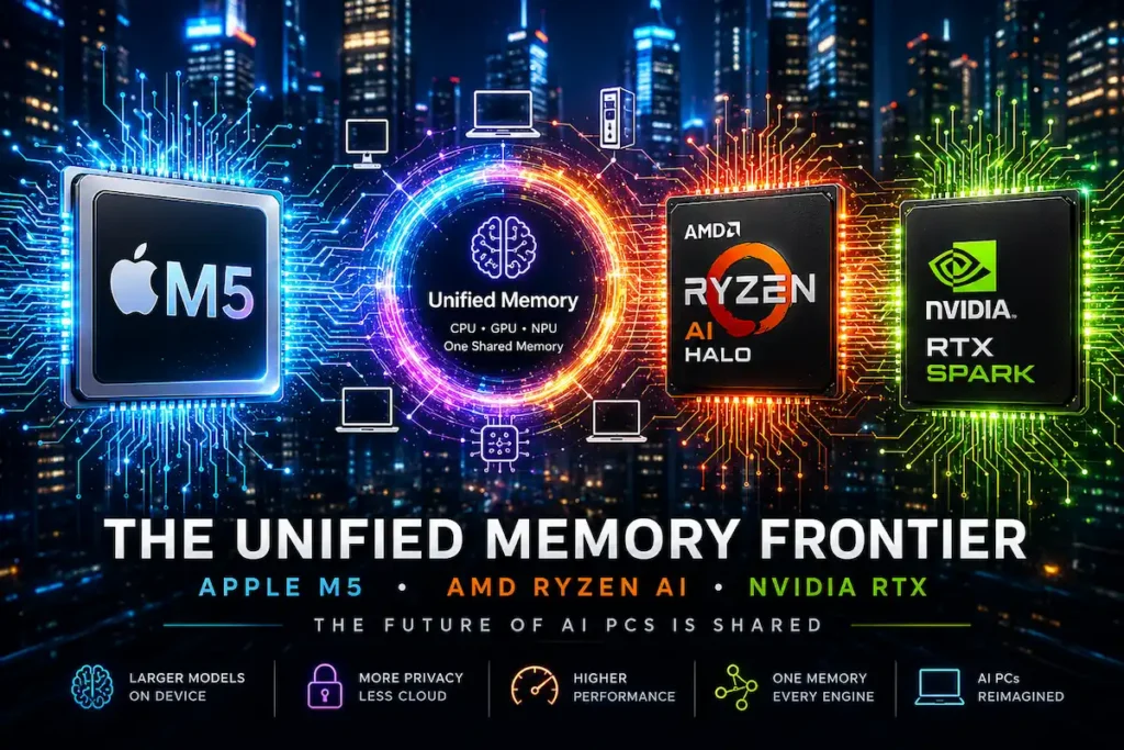 |
Unified Memory Is the Next Big AI PC FrontierApple, AMD, and Nvidia are all approaching unified memory from different directions, but the larger trend is clear: future AI PCs may depend as much on memory architecture as raw compute power. |
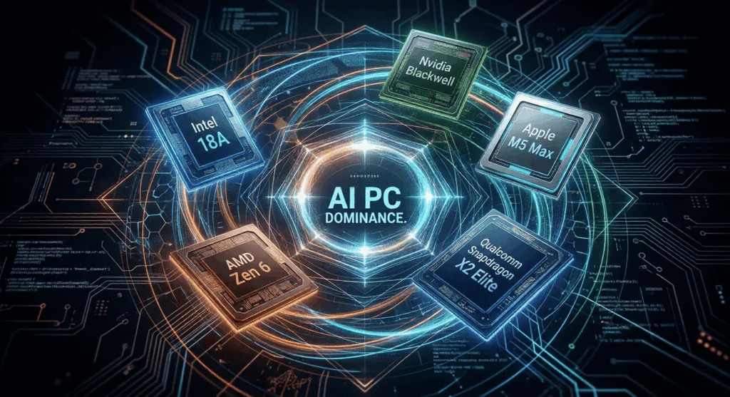 |
The 2026 Five-Way Chip War: Intel, Nvidia, Apple, AMD, and Qualcomm Battle for the AI PCThe AI PC race is no longer a two-company fight. Intel, Nvidia, Apple, AMD, and Qualcomm are all pushing different architectures as the next generation of personal computing takes shape. |