If you want to understand where the semiconductor industry is headed next, do not only watch process-node announcements. Watch fab construction, advanced packaging capacity, water access, power contracts, and the logistics required to make all of it work at once.
TSMC’s next challenge is bigger than building smaller transistors. The company is trying to coordinate a new generation of leading-edge logic manufacturing, a rapid expansion of advanced packaging, and a wider global manufacturing footprint at the exact moment AI accelerator demand is pushing the entire semiconductor supply chain to its limits.
That makes the next phase of the chip race different from the last one. For years, the headline contest was mostly about process leadership: 7nm, 5nm, 3nm, and now 2nm-class manufacturing. Those milestones still matter. But for AI chips, high-performance CPUs, custom accelerators, and future data center silicon, transistor density is only one part of the equation.
The harder question is whether TSMC can manufacture the wafers, package the chiplets, secure the substrates, qualify the tools, power the fabs, manage water needs, and replicate its Taiwan execution model across a broader global footprint.
In other words, the next silicon era may be decided as much by civil infrastructure and packaging lines as by lithography slides.
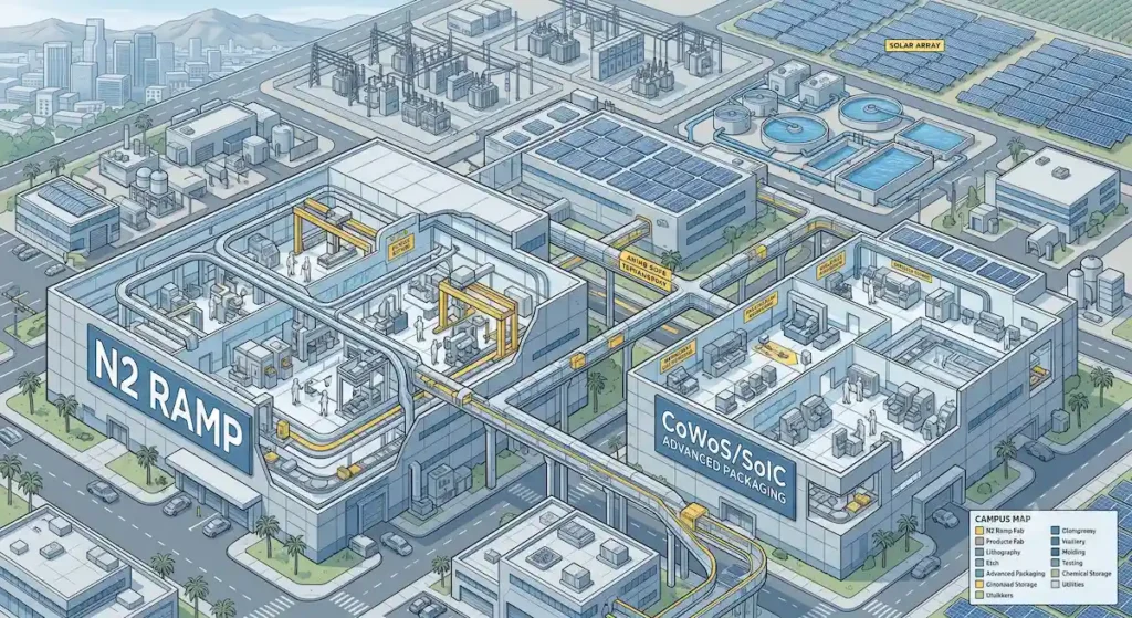
TSMC’s N2 Ramp Is Only One Piece of the Story
TSMC’s 2nm-class N2 technology represents a major technical transition because it introduces nanosheet transistors into the company’s leading-edge roadmap. TSMC says N2 entered volume production in Q4 2025, with N2P scheduled to follow in the second half of 2026. The company is also developing A16, which combines nanosheet transistors with backside power delivery for future performance and density gains.
For the average reader, the simplest way to understand this is that TSMC is not just shrinking the chip again. It is changing the transistor structure and preparing the platform for more advanced power delivery. That matters for everything from future smartphone processors to AI accelerators and high-performance computing silicon.
But the technical roadmap is only part of the story. The real challenge is scaling that roadmap across multiple fabs while customer demand remains unusually concentrated at the high end.
Apple, Nvidia, AMD, Broadcom, Marvell, and the hyperscale cloud companies all have reasons to push toward TSMC’s most advanced manufacturing options. Some need extreme efficiency for mobile devices. Others need maximum compute density for AI data centers. The pressure is coming from multiple directions at once.
That creates a synchronization problem. A new node does not become broadly useful simply because one fab can produce it. It becomes strategically important when capacity, yields, packaging, and customer design schedules all line up closely enough to support volume products.
The Old Chip Race Was About Nodes. The New One Is About Systems.
The semiconductor industry still talks in nodes because nodes are easy to market. A smaller number sounds like progress. But AI-era chips are exposing the limits of that simple story.
Modern AI accelerators are not single pieces of silicon doing everything alone. They are increasingly complex packages made from logic dies, high-bandwidth memory, interposers, substrates, chiplets, and advanced interconnects. The final product is not just a wafer-level achievement. It is a full system-in-package achievement.
That is why advanced packaging has become one of the most important bottlenecks in the industry.
TSMC’s CoWoS family of technologies is central to this shift. CoWoS, short for Chip-on-Wafer-on-Substrate, allows large compute dies and high-bandwidth memory stacks to sit together in a tightly integrated package. This is the kind of technology that makes today’s leading AI accelerators possible.
CoWoS-S uses a silicon interposer and has been widely associated with high-performance computing and AI designs. CoWoS-L uses local silicon interconnects and redistribution layers to help support larger and more complex packages. CoWoS-R leans more heavily on redistribution-layer interposer technology. The exact mix matters because each approach has different cost, scaling, yield, and supply-chain implications.
That sounds technical, but the business implication is simple: even if TSMC can produce enough leading-edge wafers, customers may still be constrained if there is not enough advanced packaging capacity to turn those wafers into finished AI processors.
Advanced Packaging Is Becoming the Real Capacity Ceiling
For AI hardware, packaging is no longer a back-end detail. It is part of the product’s performance envelope.
High-bandwidth memory has to sit close to the compute die. Chiplets need fast, reliable links. Large packages have to survive thermal stress, mechanical warpage, and power delivery demands. As accelerators grow more complex, packaging becomes more like a second manufacturing frontier.
This is where TSMC’s advantage becomes harder for competitors to copy. The company is not only leading in advanced logic manufacturing. It is also building out the packaging ecosystem needed to support that logic at scale.
That is a different kind of moat. A rival cannot simply buy a lithography tool and instantly match the whole system. It needs process integration, packaging expertise, substrate supply, testing capacity, customer trust, and years of operational learning.
This is also why Nvidia’s transition from one generation of AI hardware to the next is not only a GPU story. It is a packaging story. As AI accelerators move toward larger multi-die packages with more memory bandwidth, the industry needs more advanced packaging capacity, not just more leading-edge wafers.
That makes TSMC’s packaging expansion one of the most important semiconductor stories of the next several years.
SoIC Adds Another Layer to the Challenge
CoWoS is not the only packaging technology worth watching. TSMC’s SoIC technology, short for System on Integrated Chips, is another important piece of the company’s long-term strategy.
SoIC is associated with direct die stacking and hybrid bonding. It allows chips to be integrated vertically, not just side by side. That opens the door to denser designs, shorter connections, and potentially major performance and efficiency gains.
Consumers already see a version of this idea in products like AMD’s 3D V-Cache processors, where stacked cache can deliver major gaming performance gains. In the data center and AI world, the stakes are even bigger. Future architectures may rely more heavily on stacked logic, stacked cache, or tighter memory integration.
The challenge is that 3D stacking is difficult to scale. Thin dies, thermal density, bonding yield, and inspection all become harder when the package moves from flat integration to vertical integration. That means SoIC is strategically important, but it is not a simple capacity lever that can be pulled overnight.
For TSMC, the long-term prize is clear: combine leading-edge logic, advanced 2.5D packaging, and 3D stacking into a manufacturing platform that customers cannot easily replace.
High-NA EUV Is Important, But TSMC Is Not Treating It as the Immediate Answer
One important cleanup point in the broader semiconductor discussion is High-NA EUV. It is tempting to assume that every future leading-edge node must immediately depend on ASML’s newest High-NA EUV tools. But TSMC’s current posture appears more cautious.
High-NA EUV may eventually matter a great deal for the industry. The tools are designed to improve patterning precision and support future scaling. Intel has been more aggressive in positioning High-NA EUV as part of its future foundry strategy.
TSMC, however, has signaled that it can continue advancing near-term nodes without rushing into High-NA deployment. The reason is not that lithography does not matter. It is that TSMC appears focused on cost, maturity, throughput, and process integration rather than adopting the newest tool as quickly as possible.
That actually strengthens the broader thesis. TSMC’s edge is not just access to one machine generation. It is the ability to make thousands of process, design, packaging, and manufacturing decisions work together at scale.
The lithography race is still real. But it is no longer the only race.
Arizona Is a Test of Replication, Not Just Construction
TSMC’s Arizona expansion is one of the most visible examples of the industry’s new geography. The project has become a centerpiece of the United States’ effort to bring more advanced semiconductor manufacturing capacity onto American soil.
The question is no longer only whether TSMC can build fabs in Arizona. It can. The harder question is how quickly those fabs can approach the efficiency, cycle time, supplier density, and operational rhythm of TSMC’s Taiwan fabs.
That is a much more difficult challenge.
Taiwan’s semiconductor ecosystem is dense. Suppliers, engineers, tool vendors, materials providers, and experienced fab workers are clustered close together. That matters when a production issue requires a fast response, a tool needs service, or a process experiment needs materials quickly.
Arizona can support advanced manufacturing, but it does not yet have the same mature supplier gravity. Chemicals, specialty gases, spare parts, and experienced labor pipelines all take time to build. None of that means the project cannot succeed. It means the project is a long-term replication effort, not a quick copy-and-paste exercise.
For customers and policymakers, yield parity will be one of the most important measures to watch. If Arizona can produce advanced chips at competitive yields and cycle times, it becomes a meaningful strategic hedge. If it lags too far behind Taiwan, it still helps geographic resilience, but it does not fully duplicate Taiwan’s manufacturing advantage.
Power and Water Are Now Semiconductor Issues
The least glamorous parts of the chip story may become some of the most important.
Advanced fabs require enormous amounts of stable electricity and carefully managed water. They also need reliable wastewater treatment, chemical handling, backup systems, and grid coordination. A fab is not just a building full of tools. It is a small industrial ecosystem.
This is especially important in Taiwan, where TSMC’s core manufacturing base remains exposed to drought risk, grid pressure, and seismic concerns. The company has invested heavily in water recycling and long-term sustainability planning, but the broader point remains: leading-edge chip manufacturing is physically demanding.
The same issue applies in Arizona, where water and power questions are naturally part of the discussion. TSMC can build advanced water reclamation systems and secure long-term planning agreements, but fabs still operate in the real world. A legal water allocation is not the same thing as unlimited operational flexibility during severe drought conditions.
This is why the semiconductor race increasingly looks like an infrastructure race. The winners need engineering talent and EUV tools, but they also need substations, water systems, construction labor, permitting discipline, logistics software, and public-sector coordination.
Why This Matters for AI Chips
The AI boom has changed what “chip supply” means.
In the past, a shortage might have been mostly about wafer starts or a specific mature-node capacity crunch. Today, the shortage can appear at several layers at once. A company may have access to a leading-edge node but not enough advanced packaging. It may have packaging slots but face substrate constraints. It may have finished chips but not enough high-bandwidth memory. It may have the hardware roadmap but not the power infrastructure to deploy enough systems in data centers.
That is why AI hardware supply is so difficult to solve. The bottleneck keeps moving.
TSMC sits near the center of this entire system. It manufactures leading-edge logic for many of the most important chip designers. It provides advanced packaging for AI accelerators. It supports the design enablement work needed to bring new architectures to production. And it is now expanding across multiple geographies while demand keeps rising.
That position gives TSMC enormous leverage, but it also gives the company very little room for error.
Samsung, Intel, and Rapidus Are Chasing More Than a Node
TSMC’s competitors are not standing still. Samsung Foundry continues to pursue advanced transistor and packaging technologies. Intel Foundry is trying to use its manufacturing roadmap, advanced packaging portfolio, and High-NA EUV strategy to regain credibility with external customers. Rapidus is attempting to build a new Japanese leading-edge manufacturing option with major government support.
But catching TSMC requires more than announcing a competitive node.
The real challenge is proving that a foundry can deliver yield, volume, packaging, customer support, and roadmap confidence at the same time. That is where TSMC’s advantage remains formidable. Customers do not only buy transistors. They buy execution certainty.
For AI chip companies, that certainty is extremely valuable. Missing a production window can mean losing an entire product cycle. Delays in packaging can limit revenue even when demand is massive. Yield problems can turn a promising architecture into an expensive supply headache.
This is why TSMC’s moat is increasingly about orchestration. The company is coordinating thousands of moving parts across process technology, packaging, materials, tools, customers, and global infrastructure.
ITD Insight
TSMC’s competitive advantage has moved beyond simple process-node leadership. The company’s real moat is becoming its ability to coordinate leading-edge logic, advanced packaging, 3D stacking, customer roadmaps, utilities, suppliers, and global fab construction at the same time. In the AI era, the bottleneck is no longer just transistor density. It is manufacturing orchestration.
The Bottom Line
TSMC’s next challenge is not simply producing better chips. It is scaling a more complex semiconductor system while the AI market demands more of everything at once.
N2 and its follow-on technologies matter. CoWoS and SoIC may matter just as much. Arizona matters, but so do Taiwan’s power grid, water systems, packaging plants, suppliers, and construction timelines. High-NA EUV matters, but TSMC’s current strategy shows that tool adoption is only one part of the larger execution puzzle.
That is the deeper story behind the semiconductor roadmap. The future of computing will not be decided only by who draws the smallest transistor. It will be decided by who can turn advanced manufacturing into dependable, repeatable, global-scale supply.
The next silicon era will be built on nanosheets and advanced packaging, yes. But it will also be built on concrete, electricity, water, logistics, and the quiet operational discipline required to make impossible-looking roadmaps happen on schedule.